General Description
The Evaluation Board demonstrates the RT6252BHGJ6F to be designed for a 5V/2A output from a 4.5V to 17V input at 580kHz switching frequency. The device possesses an accurate reference voltage and integrates low RDS(ON) power MOSFETs to achieve high efficiency. The RT6252B operates in Forced PWM that helps meet tight voltage regulation accuracy requirements. The RT6252B senses both FETs current for a robust overcurrent protection (OCP). The device features cycle-by-cycle current limit protection to prevent the device from the catastrophic damage in output short circuit, overcurrent or inductor saturation conditions. The device also includes input undervoltage lockout, output undervoltage protection, and over-temperature protection (OTP) to provide safe and smooth operation in all operating conditions.
Performance Specification Summary
Summary of the RT6252BHGJ6F Evaluation Board performance specificiaiton is provided in Table 1. The ambient temperature is 25°C.
Table 1. RT6252BHGJ6F Evaluation Board Performance Specification Summary
|
Specification
|
Test Conditions
|
Min
|
Typ
|
Max
|
Unit
|
|
Input Voltage Range
|
|
4.5
|
--
|
17
|
V
|
|
Output Current
|
|
0
|
--
|
2
|
A
|
|
Default Output Voltage
|
|
--
|
5
|
--
|
V
|
|
Operation Frequency
|
|
--
|
580
|
--
|
kHz
|
|
Output Ripple Voltage
|
IOUT = 2A
|
--
|
25
|
--
|
mVp-p
|
|
Line Regulation
|
IOUT = 2A, VIN = 4.5V to 17V
|
--
|
±1
|
--
|
%
|
|
Load Regulation
|
VIN = 12V, IOUT = 0A to 2A
|
--
|
±1
|
--
|
%
|
|
Load Transient Response
|
IOUT = 1A to 2A
|
--
|
±2
|
--
|
%
|
|
Maximum Efficiency
|
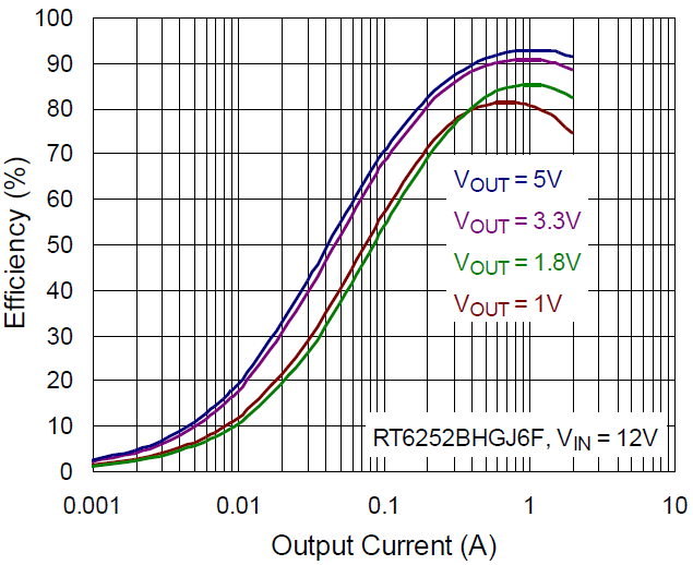
VIN = 12V, VOUT = 5V, IOUT = 2A
|
--
|
91
|
--
|
%
|
Power-up Procedure
Suggestion Required Equipments
- RT6252BHGJ6F Evaluation Board
- DC power supply capable of at least 17V and 2A
- Electronic load capable of 6A
- Function Generator
- Oscilloscope
Quick Start Procedures
The Evaluation Board is fully assembled and tested. Follow the steps below to verify board operation. Do not turn on supplies until all connections are made. When measuring the output voltage ripple, care must be taken to avoid a long ground lead on the oscilloscope probe. Measure the output voltage ripple by touching the probe tip and ground ring directly across the last output capacitor.
Proper measurement equipment setup and follow the procedure below.
1) With power off, connect the input power supply to VIN and GND pins.
2) With power off, connect the electronic load between the VOUT and nearest GND pins.
3) Turn on the power supply at the input. Make sure that the input voltage does not exceeds 17V on the Evaluation Board.
4) Check for the proper output voltage using a voltmeter.
5) Once the proper output voltage is established, adjust the load within the operating ranges and observe the output voltage regulation, ripple voltage, efficiency and other performance.
Detailed Description of Hardware
Headers Description and Placement
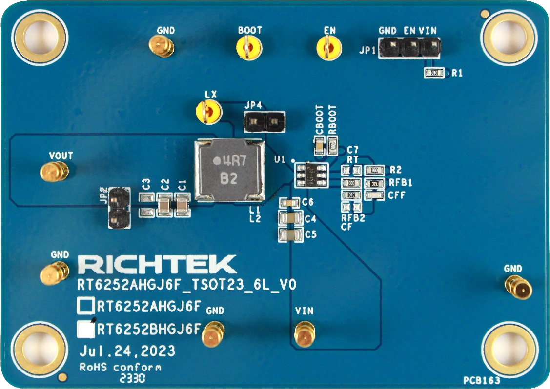
Carefully inspect all the components used in the EVB according to the following Bill of Materials table, and then make sure all the components are undamaged and correctly installed. If there is any missing or damaged component, which may occur during transportation, please contact our distributors or e-mail us at evb_service@richtek.com.
Test Points
The EVB is provided with the test points and pin names listed in the table below.
|
Test Point/
Pin Name
|
Function
|
|
VIN
|
Input voltage.
|
|
VOUT
|
Output voltage.
|
|
GND
|
Ground.
|
|
EN
|
Enable test point.
|
|
JP1
|
EN jumper. Connect EN to VIN to enable, open to disable.
|
|
SW
|
Switch node test point.
|
Bill of Materials
|
VIN = 12V, VOUT = 5.0V, IOUT = 2A, fSW = 650kHz
|
|
Reference
|
Count
|
Part Number
|
Value
|
Description
|
Package
|
Manufacturer
|
|
U1
|
1
|
RT6252BHGJ6F
|
RT6252BHGJ6F
|
Step-Down Converter
|
TSOT 23-6
|
RICHTEK
|
|
C1,C2
|
2
|
GRM219R60J226ME47D
|
22µF
|
Capacitor, Ceramic, 6.3V, X5R
|
0805
|
MURATA
|
|
C4, C5
|
2
|
GRM21BR61E106KA73L
|
10µF
|
Capacitor, Ceramic, 25V, X5R
|
0805
|
MURATA
|
|
C6, CBOOT
|
2
|
0603B104K500CT
|
0.1µF
|
Capacitor, Ceramic, 50V, X7R
|
0603
|
WALSIN
|
|
CFF
|
1
|
0603N220J500LT
|
47pF
|
Capacitor, Ceramic, 50V, NPO
|
0603
|
WALSIN
|
|
R1
|
1
|
WR06X1003FTL
|
100k
|
Resistor, Chip, 1/10W, 1%
|
0603
|
WALSIN
|
|
R2,
RBOOT, RT
|
3
|
WR06X000 PTL
|
0k
|
Resistor, Chip, 1/10W, 1%
|
0603
|
WALSIN
|
|
RFB1
|
1
|
WR06X5492FTL
|
54.9k
|
Resistor, Chip, 1/10W, 1%
|
0603
|
WALSIN
|
|
RFB2
|
1
|
WR06X1002FTL
|
10k
|
Resistor, Chip, 1/10W, 1%
|
0603
|
WALSIN
|
|
L1
|
1
|
LSXNH8080YBL4R7NJG
|
4.7µH
|
Inductor
|
L-8x8
|
TAIYO YUDEN
|
Typical Applications
EVB Schematic Diagram
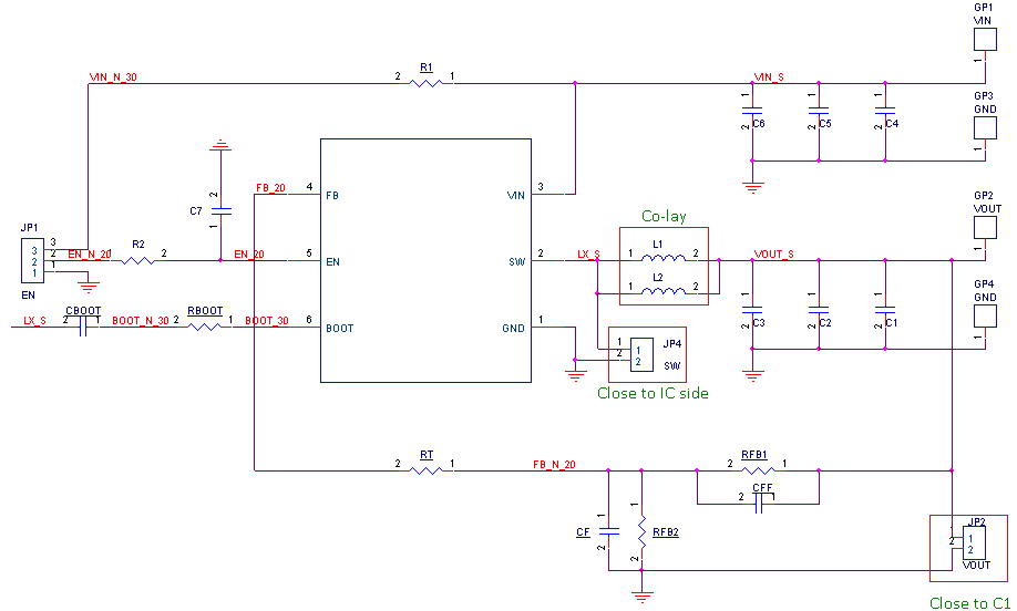
1. The capacitance values of the input and output capacitors will influence the input and output voltage ripple.
2. MLCC capacitors have degrading capacitance at DC bias voltage, and especially smaller size MLCC capacitors will have much lower capacitance.
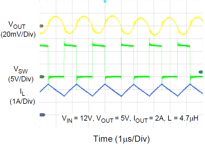
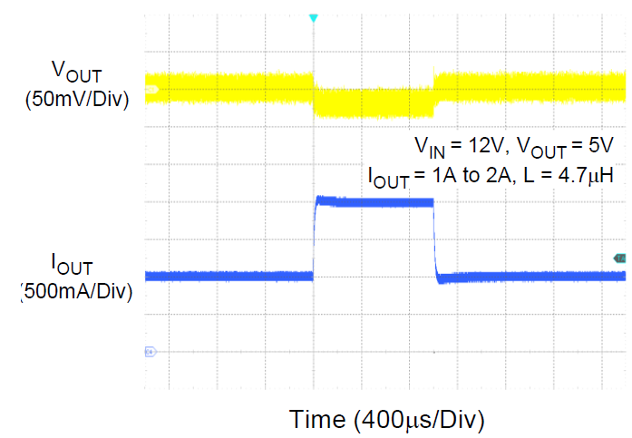
Measure Result
|
Output Ripple Measurement
|
Load Transient Response
|
|
|
|
|
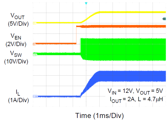
Power On from EN
|
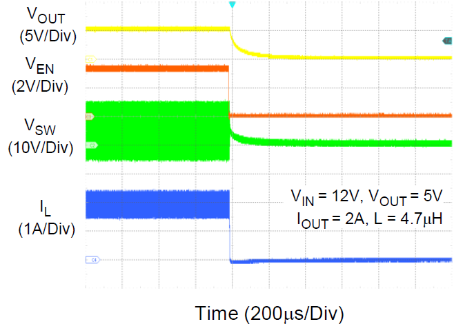
Power Off from EN
|
|
|
|
|
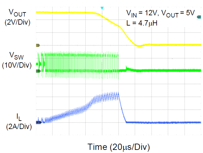
Over-Current Protection and UVP
|
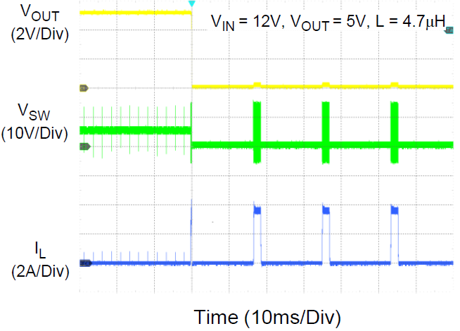
Short Circuit Protection
|
|
|
|
|
Efficiency vs. Output Current
|
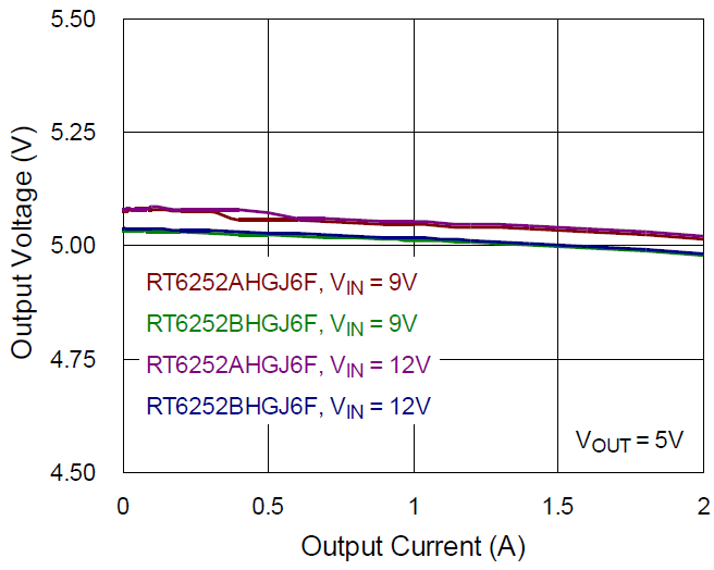
Output Voltage vs. Output Current
|
|
|
|
|
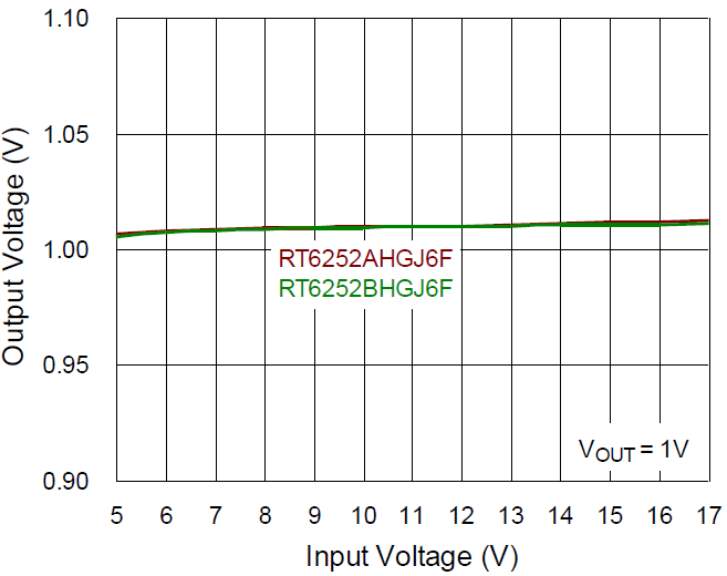
Output Voltage vs. Input Voltage
|
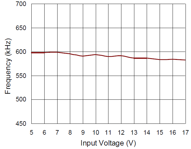
Frequency vs. Input Voltage
|
|
|
|
Note: When measuring the input or output voltage ripple, care must be taken to avoid a long ground lead on the oscilloscope probe. Measure the output voltage ripple by touching the probe tip directly across the output capacitor.
Evaluation Board Layout
Figure 1 to Figure 4 are RT6252BHGJ6F Evaluation Board layout. This board size is 70mm x 50mm and is constructed on four-layer PCB, all layers with 1 oz. Cu.
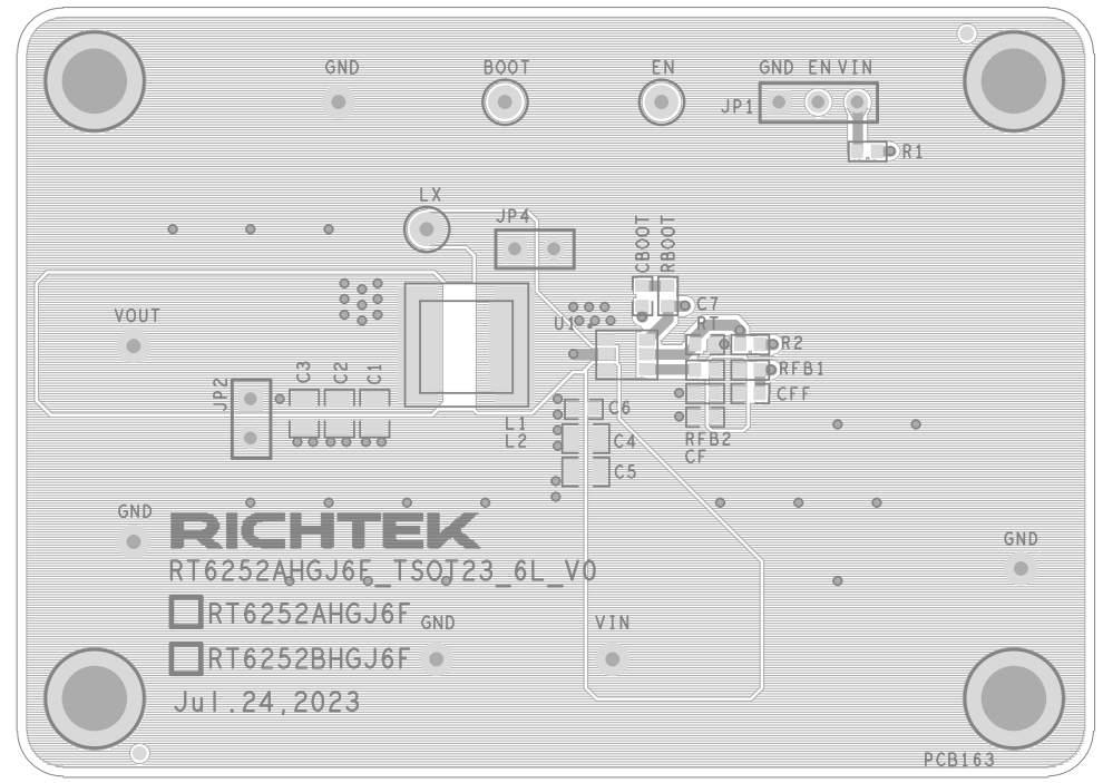
Figure 1. Top View (1st layer)
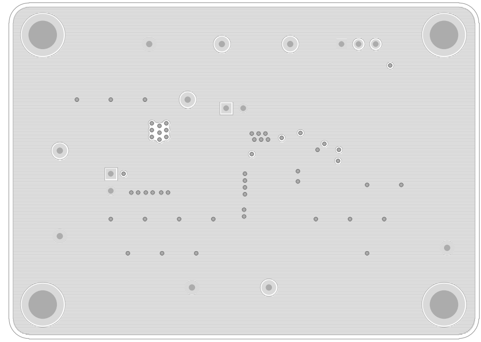
Figure 2. PCB Layout—Inner Side (2nd Layer)
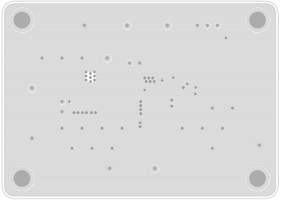
Figure 3. PCB Layout—Inner Side (3rd Layer)
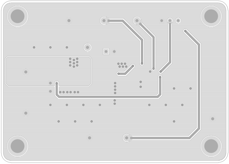
Figure 4. Bottom View (4th Layer)